Cannot create text on solder-mask layers

Bug #1788268 reported by Andrew Zonenberg
6
This bug affects 1 person
Affects Status Importance Assigned to Milestone
KiCad
Fix Released
Undecided
Andrew Zonenberg

Bug Description

Testing on 6.0.0-rc1-dev-316-ga88831d7a.

Steps to reproduce: Try to create a text object on a soldermask layer

Expected result: Soldermask layers show in the dropdown box on the layer selection dialog. This is useful for (among other things) creating layer ordering marks to ensure the right masks are used in the right order.

Actual result: Soldermask layers are not present in the dropdown.

Tags: pcbnew
Revision history for this message
Andrew Zonenberg (azonenberg) wrote :

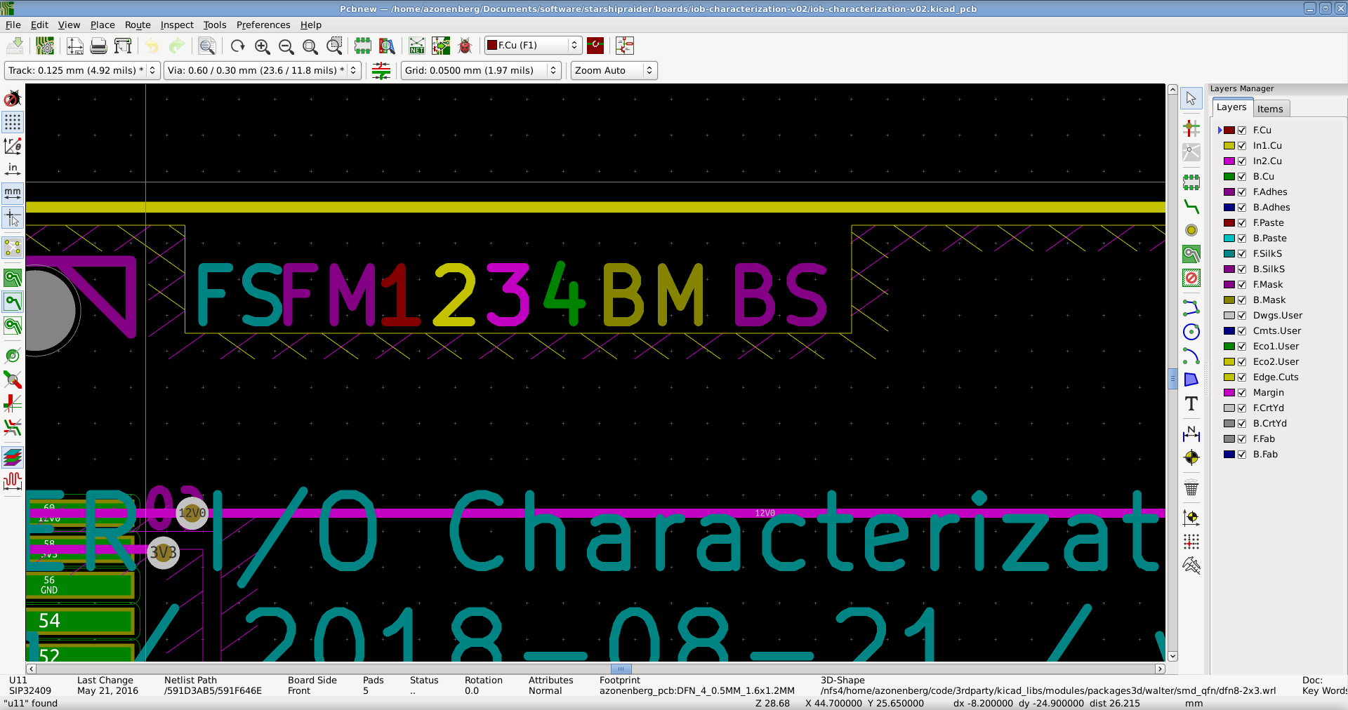
Here's an example PCB (made with an older kicad version) showing layer numbers along the top of the center edge. The "FM" text for "front mask" is no longer possible to create in current kicad.

Revision history for this message
Andrew Zonenberg (azonenberg) wrote :

Nice formatted patch combining both into one commit

Revision history for this message
Nick Østergaard (nickoe) wrote :

I was wondering when this change was introduced so I performed a git bisect with the below result. It looks like this regression is after the 5.0.0 release, that is only on current master.

ae2cb331b1dd454b4d1a66567c3ec3b7bc7f66ab is the first bad commit
commit ae2cb331b1dd454b4d1a66567c3ec3b7bc7f66ab
Author: Jeff Young
Date: Wed Jun 6 11:05:56 2018 +0100

    Merge PCBnew text edit dialogs.

    (cherry picked from commit 63b7738)

Changed in kicad:
milestone: none → 5.1.0
tags: added: pcbnew
Revision history for this message
Seth Hillbrand (sethh) wrote :

Hi Andrew-

It looks like the forbidden text layers were merged at some point during 5.1 development. This will pose some issues as the footprint text forbidden layers should be different than text forbidden layers.

In text, we only need to forbid edge cuts and margin. In footprints, we should be forbidding all copper, edge cuts, margin, paste, mask and adhesive (front/back for all).

If you're up for splitting these out, that'd be great. Otherwise, we'll get on it soon.

Revision history for this message
Andrew Zonenberg (azonenberg) wrote :

Why forbid all copper (as opposed to just internal layers) in footprints? Is there a good reason to not allow front copper text in a footprint?

Revision history for this message
Jeff Young (jeyjey) wrote :

I think we spend too much time policing the user. Why forbid text even on internal layers? Maybe the user wants to put a hidden tag in there.

@Seth, why forbid all those other layers in footprints?

Revision history for this message
Andrew Zonenberg (azonenberg) wrote :

Yeah my thought too. It makes sense to disallow text on things like edge cuts, because that is made by a milling process rather than lithography so text physically can't be created. Margin probably should be no-text too since that's used for clearance checking and text makes no real sense there.

But I'd honestly be fine with allowing text on any layer produced by litho.

Revision history for this message
Seth Hillbrand (sethh) wrote :

Copper text breaks fills and is not handled by PNS router.

Revision history for this message
Andrew Zonenberg (azonenberg) wrote :

Copper text in modules, or copper text anywhere? (The only places I use copper text are in plane cutouts, so I don't know what happens if you try to fill near it.)

Revision history for this message
Andrew Zonenberg (azonenberg) wrote :

Updated patch with separate prohibited LSET's for modules and other stuff.

Revision history for this message
Andrew Zonenberg (azonenberg) wrote :

Updated patch with indentation fixes

Revision history for this message
KiCad Janitor (kicad-janitor) wrote :

Fixed in revision 60a55d75fad8c4955b953b62f68b0b70753f3ab8
https://git.launchpad.net/kicad/patch/?id=60a55d75fad8c4955b953b62f68b0b70753f3ab8

Changed in kicad:
status: New → Fix Committed
assignee: nobody → Andrew Zonenberg (azonenberg)
Revision history for this message
Seth Hillbrand (sethh) wrote :

Thanks. Pushed with a few formatting changes and comments for the new functions

Revision history for this message
jean-pierre charras (jp-charras) wrote :

About texts in footprints on copper layers:
Any item (a footprint text in this case) on a copper layer must be handled by the DRC.

Moreover, "Why forbid text even on internal layers?"
Just because the footprint editor has no knowledge of the layers count.

Revision history for this message
Andrew Zonenberg (azonenberg) wrote :

Hmm. Because long term I would like to be able to put inner layer stuff in footprints. Maybe have a DRC error of some sort if a footprint has geometry on a nonexistent layer?

Example use case: I want to be able to make a footprint for a "4-layer stackup markings" that looks like the attached image (including a zone cutout). Right now I have to recreate that by hand in each board.

What architectural changes would have to be done to allow that?

Revision history for this message
Jeff Young (jeyjey) wrote :

@JP, but you can put text on the PCB, and DRC doesn't know any more or less about it than text in footprints, does it?

As for the footprint editor not knowing what layers are available, that's already an issue too. There's another bug report about DRC complaining because someone's board doesn't have a Front Silk layer.

I don't think either of these constraints buys us much, and they certainly get in the way of users doing what the want (such as the design in comment 17).

Revision history for this message
Andrew Zonenberg (azonenberg) wrote :

Possible fix: Allow text anywhere on the board, including footprints, but add collision checking support to DRC. To start, just do a simple bounding box around the text but potentially add more detailed geometry checking on the actual letters later.

Revision history for this message
Seth Hillbrand (sethh) wrote :

I think we have bb DRC right now.

We don't have PNS support

Revision history for this message
Andrew Zonenberg (azonenberg) wrote :

Filed a new bug (https://bugs.launchpad.net/kicad/+bug/1788699) for the lack of PNS support for copper text.

Preliminary testing indicates that both DRC and zone fills work fine with manually added text on copper layers. (Did not test with text inside footprints.)

Revision history for this message
Jeff Young (jeyjey) wrote :

We do have honest-to-god stroke-based DRC for text. It's just that it only runs on text at the board level, and doesn't dive into modules for their text.

Or I should say "used to". It's now fixed. ;)

Zone knock-outs are bounding-box-only. They too used to only look at text at the board level. That's also now past-tense.

These fixes also improve the anchor locations to the actual collision location (for both PCB text and footprint text).

As Andrew discovered the PNS router doesn't handle text at all: PCB text or otherwise. So that's irrelevant to this discussion; we'll leave it for the bug he logged.

Any objections to me re-unifying the PCB & Module forbidden layer sets?

Revision history for this message
Seth Hillbrand (sethh) wrote :

I think we need to wait to update the file format to allow footprints access to inner layers.

Revision history for this message
Andrew Zonenberg (azonenberg) wrote :

@Seth: Once #1788699 is fixed, any objection to me re-enabling front copper text in footprints? Seems like that's the last remaining blocker.

We can worry about other copper layers later.

Revision history for this message
Jeff Young (jeyjey) wrote :

I don't think we need to wait for 1788699 -- PNS is just as broken with PCB copper text which we already allow.

Inner layers in footprints is kind of a different issue: they currently don't show up because the footprint editor board is a two-layer board, not because they're forbidden. I'm fine with leaving it a two-layer board for now.

Revision history for this message
Seth Hillbrand (sethh) wrote :

No objections here.

Revision history for this message
Wayne Stambaugh (stambaughw) wrote :

If this breaks compatibility with 5.0, it will have to be removed. Please test it with 5.0 to make sure any files created with this change, can be opened and modified with 5.0.

Revision history for this message
Franck78 (fbourdonnec) wrote :

From pcb_calculator to track calculator....

-Copper text
-Antennas, inductance
-Filters
-Bus with of varying size
-Net ties
-Surge protectors

The common point between all of those things is *COMPONENT MADE OF TRACKS SEGMENTS*

Make the necessary changes to make a component represented by tracks
-add the possibility to make the object just drawn OR
-call a formula that return the shape of the track. Because this is an advanced method, all parameters are passed with one field same as a URL with params. No GUI needed for each object. Just formulas write by skilled engineers.

For example, requesting a Tie for 3 nets will return a calculated footprint with three pads
VirtualCOMPONENT:Tie() (the formula to call)
REF:shape=rectangle;nets=Xyz,Abc,Def;......

If I'm not wrong, DRC is not bothered by components. A zero ohm resistors on two nets is not checked. So for this calculated component.
For Copper text, it's a component, not a lost piece of copper

You get the idea. Some component are added in schema editor. Some properties can trigger a calculated component, the thing is : no fixed footprint.

Revision history for this message
Andrew Zonenberg (azonenberg) wrote :

@Wayne: Text on soldermask layers used to work in 5.0 and I have many physical boards fabbed with it. ae2cb331b1dd454b4d1a66567c3ec3b7bc7f66ab introduced a regression which broke compatibility with boards containing text on soldermask. 60a55d75fad8c4955b953b62f68b0b70753f3ab8 fixes this and restores the previously-working functionality.

Revision history for this message
Wayne Stambaugh (stambaughw) wrote :

@Andrew, thanks for the update. Please, ignore my previous comment.

Changed in kicad:
status: Fix Committed → Fix Released
To post a comment you must log in.
This report contains Public information  
Everyone can see this information.

Other bug subscribers

Remote bug watches

Bug watches keep track of this bug in other bug trackers.